Power Designs Inc 6050C Display Mod

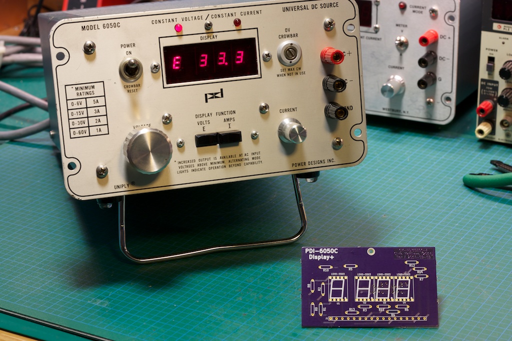
Here’s a modification that I have been meaning to do for a while. It involved replacing the PCB in one of my power supplies with a modified version designed by me that upgraded the size of the 7-segment LED display.

IMG_5736

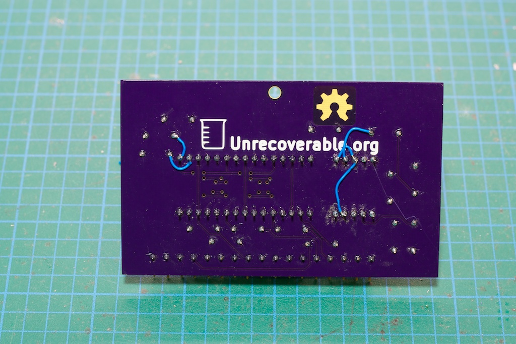
I ordered the board from OSHPark. My experience with them has been positive; the turn around time was about 2 weeks and the gold finish is very nice. I’m fine with the colour of the solder mask, however note that the mask is a matte finish rather than the typical “pearl” or “glossy” finish that I am accustomed to seeing on PCBs. Not a big deal, but something to think about. Also, the traces are a bit difficult to see through the solder mask.

IMG_5737 IMG_5739 IMG_5741

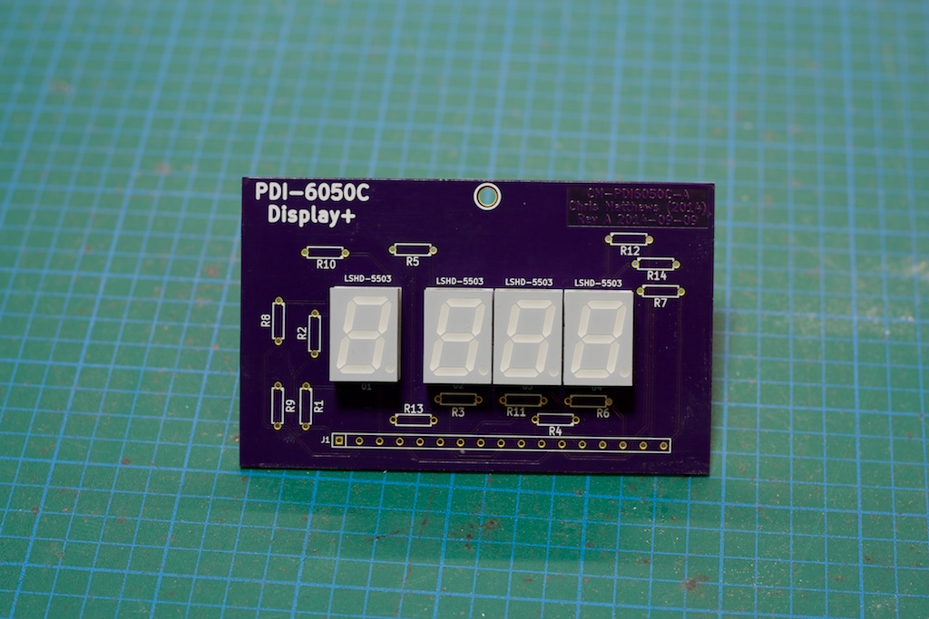
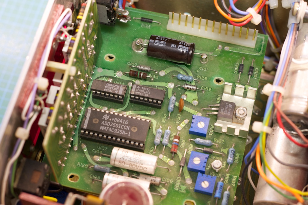
I of course did not fully check my notes when throwing together the schematic for this project which resulted in the boards I received having the ‘a’ and ‘g’ segments reversed. A few cut traces and a jumper wires later and all was working as expected.

IMG_5745 IMG_5744  IMG_5742IMG_5743

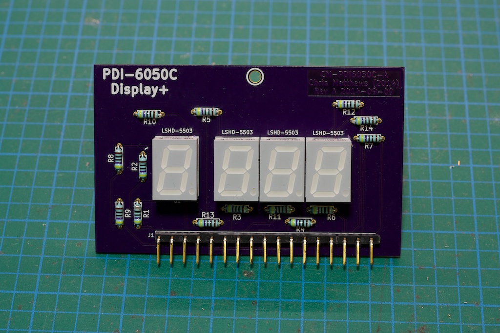
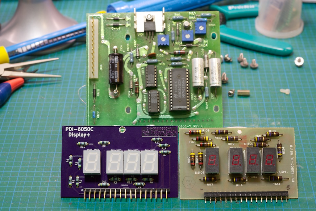
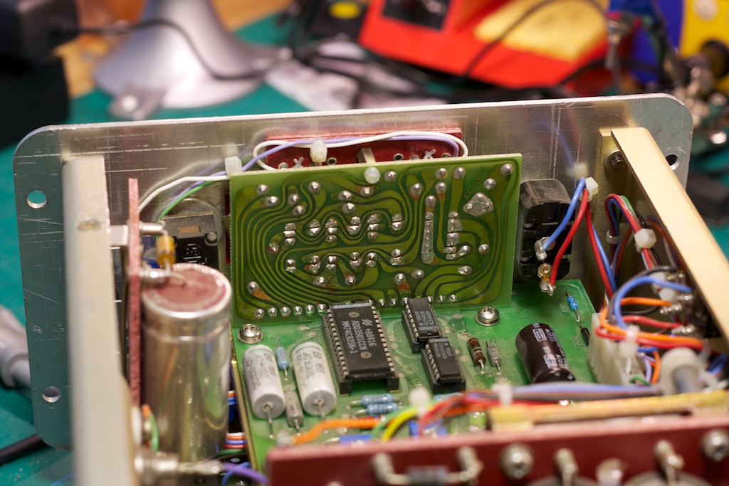
I originally tried to think of a better way of re-attaching the new display board to the existing display measurement/logic board, but in the end the simplest solution won out and  I just re-soldered the new display board back. The header pitch is 3.81mm and was a total pain to find (yay eBay!).

IMG_5746

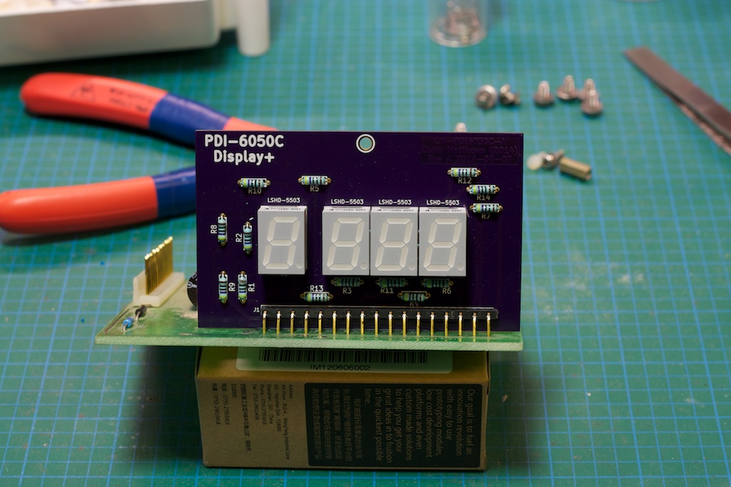
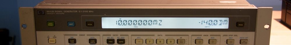
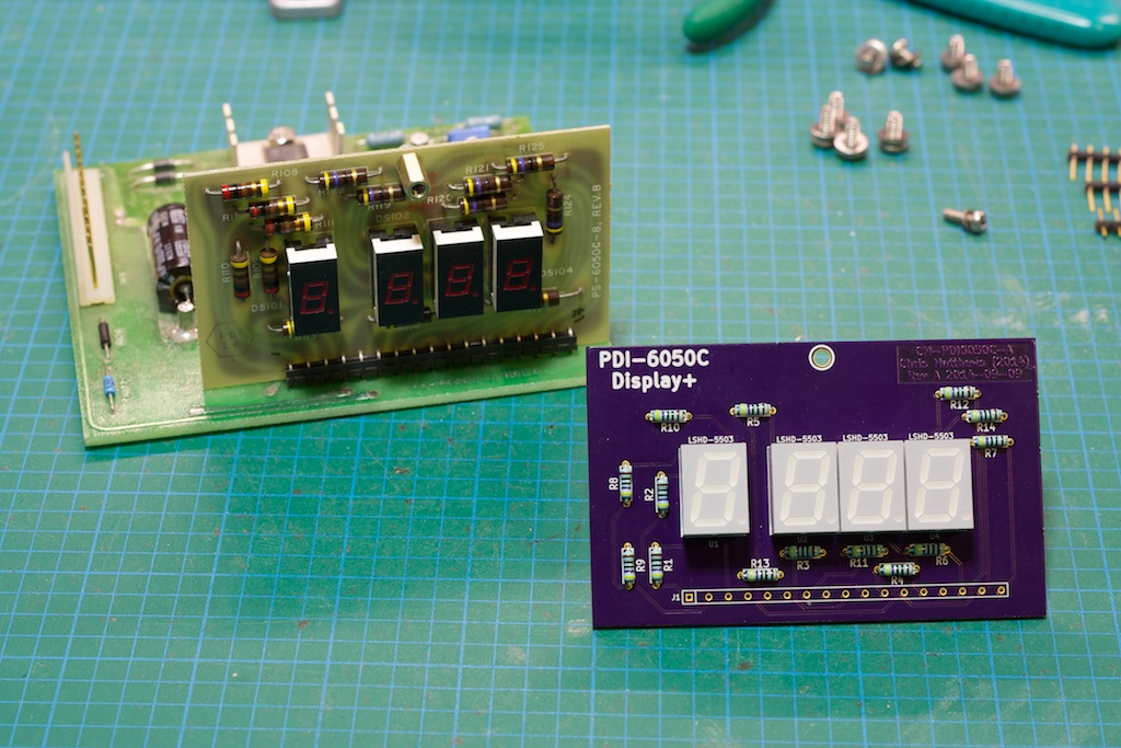
The end result is a bright, clear and LARGER display. Here I have contrasted it with the model right after the 6050C, the 6050D which has a larger digital display (and also does not display the measurement mode as the 6050C does, E or I).IMG_5748
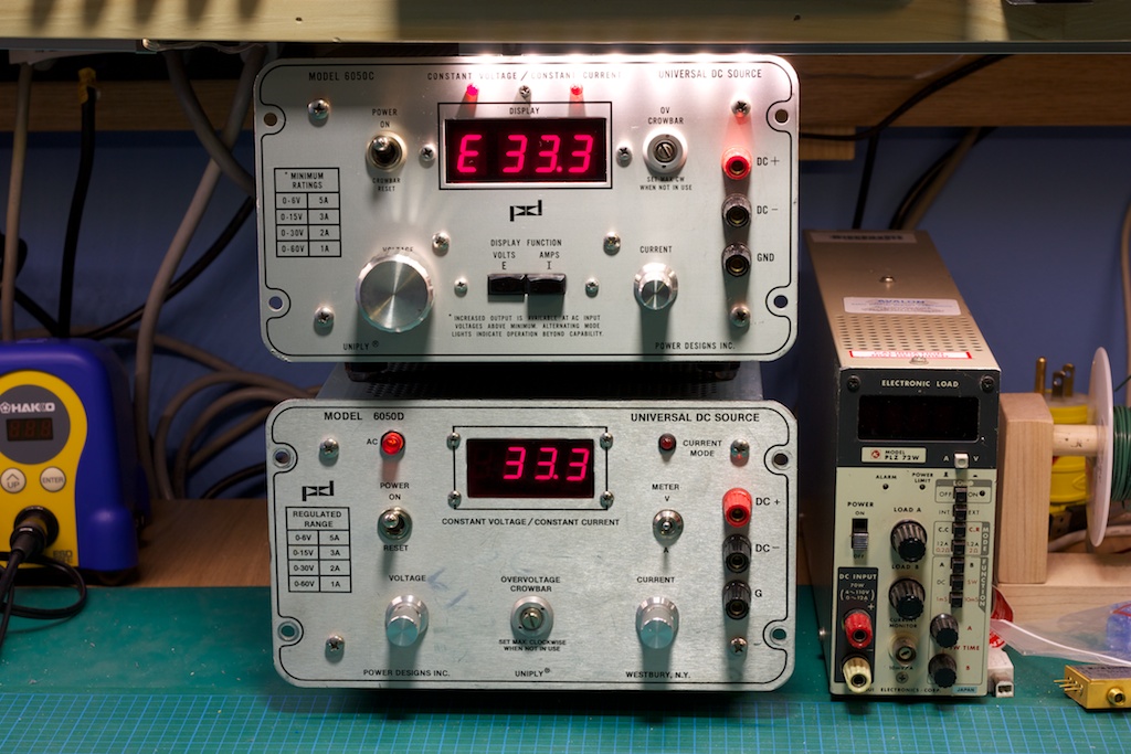
If I decide to pick up any more of these supplies, I think I’d make the same display modification to them as well. I have been looking at the 6050A models (which can usually be had for cheaper): these might also be good for a “digital makeover” involving removing the analog meter and designing a new digital display PCB.


USB to Serial Adapter Project

Not satisfied with the “typical” USB to serial cables that one can readily buy, I decided to design my own.  The basic reason was just another excuse to practice designing a circuit and laying out a printed circuit board (PCB), but to also create a very small unit that can be easily transported. I additionally wanted to have some sort of visual feedback of data transfer over the adapter, so two LED’s (receive and transmit) will address that.

The circuit design came from the application notes on the FTDI chip that I am using, the FT230X:

USB2Serial

I did a few tests with a bread-boarded version of this circuit. You will notice that there are 2 bread boards; the bottom one has the USB to serial circuit, the top one has an Atmega8 micro-controller with a some program that echoes back characters it receives on its serial interface (used for testing):

IMG_5304


A close-up of the USB to serial circuit:

IMG_5308

And the two circuits/bread-boards separated:IMG_5307

The other requirement was size: that whole circuit will need to fit within this little box:

IMG_5309

I have actually laid out the board, and so will be finalizing it in the coming days. I will write up another post with the board layout, 3D shots and a bill of materials. In terms of price, this will not be saving me any money over buying a pre-built adapter.

Board Update

Just as a quick followup, I have received my first circuit board in the mail today, and I must say, I am kinda impressed at the quality of the work done in producing the boards.  I give much thanks and props to the people at iTead Studio:

IMG_5088

And a little comparison with our long friend (this will date this post if anything will):

IMG_5089

There are couple of little issues with the board, but none of them are due to the manufacturer, just due to my in-experience 🙂  So ~20 boards for $63 shipped and delivered in about 2 weeks.  Pretty good 🙂

First ever board!

This past week has seen a first for me: I created a prototype for a simple controller board for a motor, created a Printed Circuit Board (PCB) design from this schematic and then sent it off to be manufactured by iTeadStudio. Here are a couple of top/bottom shots of the 3D view of the board from Kicad:

MosfetDriverBoard-top MosfetDriverBoard-back

I will post an update after I receive the boards back from the manufacturer, along with pictures. I can hardly wait! 😀