It is said that one should learn from one’s mistakes. In the process of learning how to design and get a Printed Circuit Board (PCB) manufactured, I have indeed made a few mistakes. I would like to share them with you here.
First, a quick update on the board that I was designing. My requirement was to be able to drive a spinning light assembly (pictured below) from a micro controller (MCU). Rather than use the traditional relay-based system (which would use a transistor to achieve MCU control) I decided to design it using a MOSFET (a big ‘ol voltage-controlled switch). I also figured that this would present a good opportunity to learn how to design and lay out a very simple PCB.
Always, ALWAYS, Double-Check Your Work
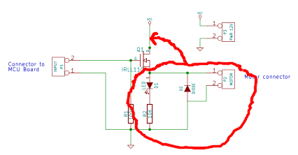
I don’t know if I can emphasize this more: a core theme in all of my mistakes during this project have been due to this. My first board, Rev ‘A’, suffered from a major circuit design error that occurred when I moved my circuit design from the bread board to the schematic CAD tool (I got the circuit backwards: I needed one that worked with a “NPN” transistor, but designed one that worked only with a “PNP” transistor).
Here is my awesome not working circuit (Rev A):
Here is the corrected circuit with the motor BEFORE the NPN MOSFET:
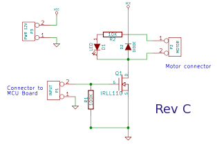
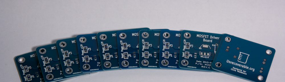
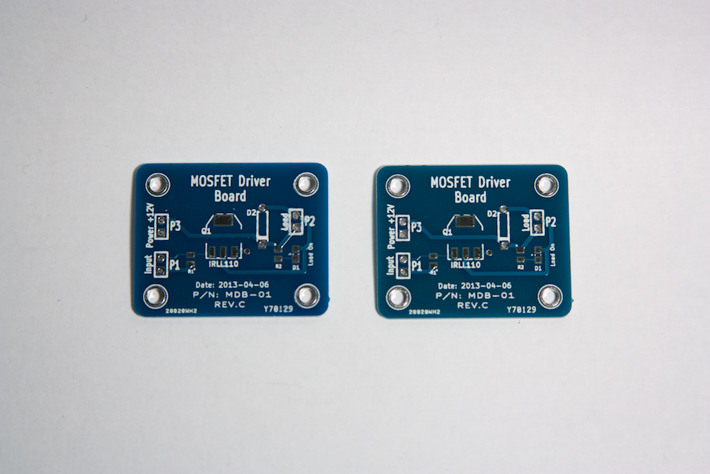
My second revision, Rev ‘B’, was not manufactured; it had the corrected circuit design, but I wanted to tighten up the physical PCB layout so I created Rev ‘C’:
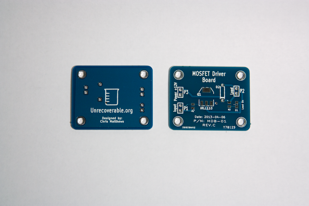
I had this revision manufactured. The mistake that I should have caught on this time was the adjustments I had made to the hole diameters for the terminals (for the inputs and outputs); I had forgotten to adjust the copper (called “annular ring”) around the holes to make them larger as well. This wasn’t a show stopper, as I was able to solder the components on the board still, but it was borderline.
As an aside, I noticed that the front solder-mask (the blue color) was not uniform between boards; some were blue and others were slightly blue-greenish, about half and half. I also noticed that the silk-screening was less than awesome on all the boards. Note that this board was Hot Air Solder Leveled (HASL) and NOT gold plated like the first revision board.
Thou Shall Check The Data Sheet. Again.
The second biggest mistake that I made was not re-checking the foot prints (the “physical” sizing of a component) during and after I completed the layout of the PCB. DO THIS. It avoids embarrassing mistakes such as holes that are too small to fit the leads of a through-hole component. You should also re-check the pad/leads in the data sheets to make sure they fit with your component symbols and circuit design. Don’t assume anything!
Always Have a Reason
When you place a component, connect a trace, add a connection, always have a reason for doing so! This will prompt you to ask yourself why you are doing this and perhaps lead you to discover a mistake in the making.
Test Points
This board was a bit too small to warrant test points (PCB pads that are designed specifically to be accessible to probes for testing properties of your circuit) but remember to think about adding them in. This can make debugging a malfunctioning circuit much easier later on. Also remember that it may be a good trade-off when designing a prototype device to take a little more space but offer debugging facilities such as test points and wire jump points.
Remember To Add Your Name!
If you truly are happy with your design and PCB layout, then you won’t mind putting your name, date, revision information and other useful identification information on the PCB. Do it! This will make differentiating board revisions easier as well as identifying you as the designer. Take some credit!